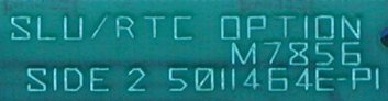
DL11-W SERIAL LINE UNIT (SLU)
REAL-TIME CLOCK |
M7856
|
INTRODUCTION
The DL11-W (M7856) is a UNIBUS quad-height interface that offers one serial input line, one serial output line, and
a so-called real-time clock.
Its name is often abbreviated to "SLU / RTC", which stands for Serial Line Unit / Real-Time Clock.
On this page you can find the following information.
If you want to print this page on A4 or Letter format, set the scaling in the printer driver to 80%.
AVAILABLE DOCUMENTATION
- Manuals
-
- DL11-W serial line unit/real-time clock option operator's manual (EK-DL11W-OP-001)
- Engineering drawings
-
- DL11-W Field Maintenance Print Set MP00106 (rev. B)
MODULE DESCRIPTION
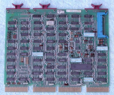
The DL11-W provides two functions. First, the module is a character-buffered communications interface that has two independent
units (receiver and transmitter) capable of simultaneous 2-way communication. Second, the DL11-W has a line frequency clock (50 or 60
Hz.) that can generate timed interrupts. The functionality of the module is set by five DIP switch packages and the wiring of the
BERG connector on the module. Click the image to identify the DIP switch packages S1 thru S5.
The DL11-W can replace the DL11-A, DL11-B, DL11-C, and DL11-D modules in most applications. All of the DL11-A thru DL11-D features
are switch-selectable available on the DL11-W. The DL11-W supports the following interface.
- 20 mA current loop (passive mode)
- 20 mA current loop (active mode)
- EIA RS-232
The module has the following power requirements.
- +5V at 2.0 A.
- -15V at 150 mA.
- +9 ... +15V at 50 mA.
(only required if the EIA level outputs are used)
MODULE CONFIGURATION
As the DL11-W is such a versatile serial line module, the configuration can best be handled in the following steps.
- Set the UNIBUS address and vector for the SLU and LTC.
- Set the baudrate for the receiver and the transmitter section.
- Set the character properties (# bits, stopbit length, parity)
- Set the interface properties (current loop active/passive mode or EIA)
- UNIBUS side
-
The DL11-W can be used in 3 different modes :
- Serial Line Unit and Line Time Clock
- Serial Line Unit only
- Line Time Clock only
| Mode | S5-9 | S5-10 |
|---|
| 1 | OFF | ON |
|---|
| 2 | ON | OFF |
|---|
| 3 | ON | ON |
|---|
As the address decode logic on the module is common for the serial line and the Line Time Clock, and the Line Time Clock
address is fixed set at 777546, it restricts mode 1 (serial line and LTC) to the address range 77756x. Mode 3 has also
a fixed vector number, 100. You can install up to 47 DL11-W modules in a system, but only one DL11-W can have the LTC enabled,
the LTC must be disabled on all other DL11-W's in the system. The operation mode is defined by the setting of two DIP
switches of package S5, S5-9 and S5-10.
The UNIBUS address is defined by the other eight DIP switches of package S5, S5-1 thru S5-8.
| Address bit | A10 | A9 | A8 | A7 |
A6 | A5 | A4 | A3 |
|---|
| DIP switch | S5-3 | S5-2 | S5-1 | S5-4 |
S5-5 | S5-6 | S5-8 | S5-7 |
|---|
| system console |
OFF | OFF |
OFF | ON |
OFF | OFF |
OFF | ON |
|---|
| TU58 emulation |
OFF | ON |
OFF | ON |
OFF | ON |
ON | ON |
|---|
| Note. "OFF" = logic '1' ! |
The system console is shown as an example, as it is a very common setting. The system console is always at address 777560. As this
address is in the range of the LTC, it is very common to have the LTC enabled on the system console interface. The second example
defines the standard address for the TU58 device "DD" at address 776500.
| Data bit | D8 | D7 | D6 | D5 | D4 | D3 |
|---|
| DIP switch | S2-8 | S2-7 | S2-5 | S2-3 | S2-6 | S2-4 |
|---|
| system console |
OFF | OFF | OFF |
ON | ON | OFF |
|---|
| TU58 emulation |
OFF | ON | ON |
OFF | OFF | OFF |
|---|
| Note. "ON" = logic '1' ! |
The vectors for the system console is 060 for the receiver and 064 for the transmitter section.
The vectors for the TU58 device are 300 and 304.
Remark. DIP switch 1 and 2 of S2 are not used.
- Baudrate receiver / transmitter
-
| Baudrate | Transmit | Receive |
|---|
| S4-10 | S3-1 | S3-4 | S3-2 | S3-3 | S3-5 |
|---|
| 110 |
ON | ON | ON |
OFF | OFF | OFF |
|---|
| 150 |
OFF | ON | ON |
ON | OFF | OFF |
|---|
| 300 |
ON | OFF | OFF |
OFF | ON | ON |
|---|
| 600 |
ON | OFF | ON |
OFF | ON | OFF |
|---|
| 1200 |
ON | ON | OFF |
OFF | OFF | ON |
|---|
| 2400 |
OFF | OFF | OFF |
ON | ON | ON |
|---|
| 4800 |
OFF | OFF | ON |
ON | ON | OFF |
|---|
| 9600 |
OFF | ON | OFF |
ON | OFF | ON |
|---|
You can set the baudrate of the receiver and the transmitter section independent of each other.
As already seen, when you set the DIP switches for the address and vector, the DIP switches are not placed in a logical order.
Three DIP switches of package S3 set the baudrate of the receiver section. Two more DIP switches of package S3 set the baudrate of the
transmitter section and one DIP switch of package S4 ...
- Character properties
-
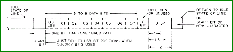 The character properties are the following, and are all set by five DIP switches of the package S4.
The DIP switch positions 8 and 9 of the package S4 are not used.
When you set the DIP switch position 1 of the package S4 to "ON" the transmitter sends continuously a
BREAK.
When you set the DIP switch position 7 of the package S4 to "ON" the error bit is enabled.
- Number of data bits
| # data bits | S4-4 | S4-3 |
|---|
| 5 | ON | ON |
|---|
| 6 | ON | OFF |
|---|
| 7 | OFF | ON |
|---|
| 8 | OFF | OFF |
|---|
The number of data bits is set by two DIP switches of package S4.
- Bit-time of the stopbit
The length of the stopbit is set by one DIP switch of package S4, S4-5.
When S4-5 is "OFF" the length of the stopbit is one bit time.
When S4-5 is "ON" the length of the stopbit is two bit times when the number of data bits is 6, 7, or 8,
and the length of the stopbit is 1� bit times when the number of data bits is 5.
- Parity bit options
| Parity bit | S4-6 | S4-2 |
|---|
| disabled | OFF | * |
|---|
| even parity | ON | OFF |
|---|
| odd parity | ON | ON |
|---|
The parity bit is set by two DIP switches of package S4.
You can select even or odd parity, and you can disable the parity.
If the parity bit is disabled, the bit is not transmitted, and the parity of a received character is not checked.
The asterisk (*) means that the position of the DIP switch is "don't care".
- Interface properties
-
The interface can be set to EIA level (RS-232) or 20 mA current loop.
When the interface is set to 20 mA current loop, you can define whether the current for the loop is provided by the DL11-W
(called 'active mode'), or that the connected device supplies the current for the loop (setting on DL11-W to 'passive mode').
Note that the choice of current loop or EIA levels is selected by the connection of the wires on the BERG connector.
DIP switches of the packages S1 and S3 define the active/passive mode of operation of the transmitter, the receiver, and the
paper tape Reader Enable loops when the interface is used in a current loop.
| mode |
Transmitter | Receiver |
Paper tape Reader Enable |
|---|
| |
S1-1 | S1-2 | S1-3 | S1-6 | S1-7 |
S3-6 | S3-7 | S3-8 | S3-9 | S3-10 |
S1-4 | S1-5 | S1-8 | S1-9 | S1-10 |
|---|
| active |
ON | ON | OFF
| OFF | ON |
ON | OFF | ON
| OFF | ON |
ON | OFF | ON
| OFF | ON |
|---|
| passive |
OFF | OFF | ON
| OFF | ON |
OFF | ON | OFF
| ON | OFF |
OFF | ON | OFF
| ON | OFF |
|---|
MODULE CONNECTION
- UNIBUS
You can install the DL11-W in any SPC (Small Peripheral Controller) slot of a 4-slot DD11-CK of 9-slot DD11-DK backplane.
Note that the M7856 module does not use, nor connect the NPG connection. If you install the
M7856 module in an SPC slot, make sure that the NPG chain is wired on the backplane (or the DIP switch for the slot in which
the M7856 module is installed is closed on the MDM module in the PDP-11/84 and 11/94). If you do not want to "mess around"
on the backplane, you can solder a wire on the component side of the module to connect CA1 to CB1. If you are not sure which
contact fingers to connect, use the G7273 NPG / Grant Continuity module as an example.
- PERIPHERAL DEVICE
The peripheral device is connected to the BERG header on the DL11-W module.
On this BERG header connector all signals are available, such as
- serial data input at TTL logic level, at EIA level, and (pos/neg) for 20mA current loop
- serial data output at EIA level, and (pos/neg) for 20mA current loop
- Data Terminal Ready output at EIA level
- Request to Send output at EIA level
- Reader Run (pos/neg) for 20mA current loop
On the BERG header are also several connections called "interlock" that actually define the type of interface, EIA or current loop.
The green fields in the table are the EIA signal, the blue fields are the 20 mA current loop signals.
| BERG pin | signal |
BERG pin | signal |
|---|
| A | Ground |
B | Ground |
| C | |
D | |
| E | Serial input (TTL) |
F | Serial output (EIA) |
| H | 20 mA Interlock |
J | Serial input (EIA) |
| K | + Serial input (20 mA) |
L | |
| M | EIA Interlock |
N | |
| P | |
R | |
| S | - Serial input (20 mA) |
T | |
| U | |
V | Request to Send (EIA) |
| AA | + Serial output (20 mA) |
BB | |
| CC | |
DD | Data Terminal Ready (EIA) |
| EE | - Reader Run (20 mA) |
FF | |
| HH | |
JJ | |
| KK | - Serial output (20 mA) |
LL | |
| MM | |
NN | |
| PP | + Reader Run (20 mA) |
RR | |
| SS | |
TT | +5 Volt |
| UU | Ground |
VV | Ground |
Plug and interlock wiring
When you look at the table of the connection pins of the BERG header, it is almost a trivial task, but to get the wiring
working you must make an "interlock", basically a short between two pins.
- Wiring as DTE for EIA (RS-232) to a terminal (e.g. VT100) [DB25 male]
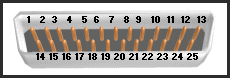 Use the pin A, or VV as connection to Ground (DB25 pin #1).
Use the pin B, or UU as connection to Ground (DB25 pin #7).
Serial data in (pin J) to RXD (DB25 pin #3).
Serial data out (pin F) to TXD (DB25 pin #2).
Request to Send (pin V) to RTS (DB25 #4).
Data Terminal Ready (pin DD) to DTR (DB25 pin 20).
Connect an short wire between the EIA Interlock pin M and the Serial input TTL pin E.
Remark. RTS and DTR can not be controlled (hardware-wise always active).
- Wiring for 20 mA current loop to a terminal (e.g. VT220) [Mate-N-Lok]
Serial output [-] (pin KK) to Mate-N-Lok pin #2.
Serial output [+] (pin AA) to Mate-N-Lok pin #5.
Serial input [-] (pin S) to Mate-N-Lok pin #3.
Serial input [+] (pin K) to Mate-N-Lok pin #7.
Reader Run [-] (pin EE) to Mate-N-Lok pin #3.
Reader Run [+] (pin PP) to Mate-N-Lok pin #6.
Connect an short wire between the 20 mA Interlock pin H and the Serial input TTL pin E.
MODULE TEST
For a thorough test there is nothing better than the XXDP program ...
However, a few simple tests can tell you if the module transmits a character and receives a character. In the following example,
I use the addresses that are reserved for the system console. When the base address of the module is set to 777560, the registers
for the serial communication channel are mapped to the following locations :
- 777560 - RCSR , receiver status register
- 777562 - RBUF , character receive buffer
- 777564 - XCSR , transmitter status register
- 777566 - XBUF , character transmit buffer
Check that the switches of the DIP switch packages are in the correct position, and make a note for future reference ...
Check with an Ohm meter or a beeper that the closed DIP switches are actually closed! They might be stuck internally,
and that is usually in the "open' position. If you find a a bad switch, click the bad switch a dozen time in each direction
back and forth, with a couple of small screwdrivers or pencils (one in each dimple on the switch) until the switch operates
reliable.
This setup description uses the EIA (RS-232) interface.
Connect a simple 3-wire cable to the BERG header of the module. Connect the pins B, F, and J to the connector for the terminal,
and connect the interlock wire between the pins E and M. The PDP-11's do not use any handshake signals (at least not for the system
console), so the simple 3-wire cable is all you need to connect a terminal like the VT220. If you connect the DL11-W to the COM#: port
of a PC and use a Terminal Emulation application program on the PC, the PC might need the proper levels at its handshake pins.
Make sure that the baudrate, stopbit, parity and number of data bits match between the DL11-W and the terminal (application).
- After you initialised the PDP-11, (bus INIT, reset, whatever you want to call it), the 777560 RCSR register should contain 000000.
- The next test is the reception of a single character. Press (for example) the number "6" key on the keyboard of the terminal. Then ...
- EXAMine the receiver status register 777560.
It should have bit 7 set (value is 000200), which indicates that the receiver did receive a character.
- EXAMine the receiver buffer 777562, the data should be 66 octal (if you pressed the number "6" key on the
keyboard).
If any of the 4 upper bits of the word at 777562 is set, an error occurred.
- The last simple test is DEPosit an ASCII character in the transmit register 777566, for example (octal) 63.
The moment you deposit that value, you should see the number "3" appear on the terminal (if you deposited octal 63).